- Company
회사소개
- 주식회사 나노시스템을 소개합니다.
- Product
제품소개
- 주식회사 나노시스템의 제품을 소개합니다.
- Technology
기술 및 적용분야
- 나노시스템에 기술을 확인하세요.
- Career
인재채용
- 나노시스템은 능력있는 당신을 기다립니다.
- Contact Us
문의사항
- 문의사항
- News&Notice
나노시스템 소식
- 나노시스템 소식을 확인하세요.
회사소개
제품소개
기술 및 적용분야
인재채용
문의사항
나노시스템 소식
The World-Class Leading Company in Measurement and Inspection
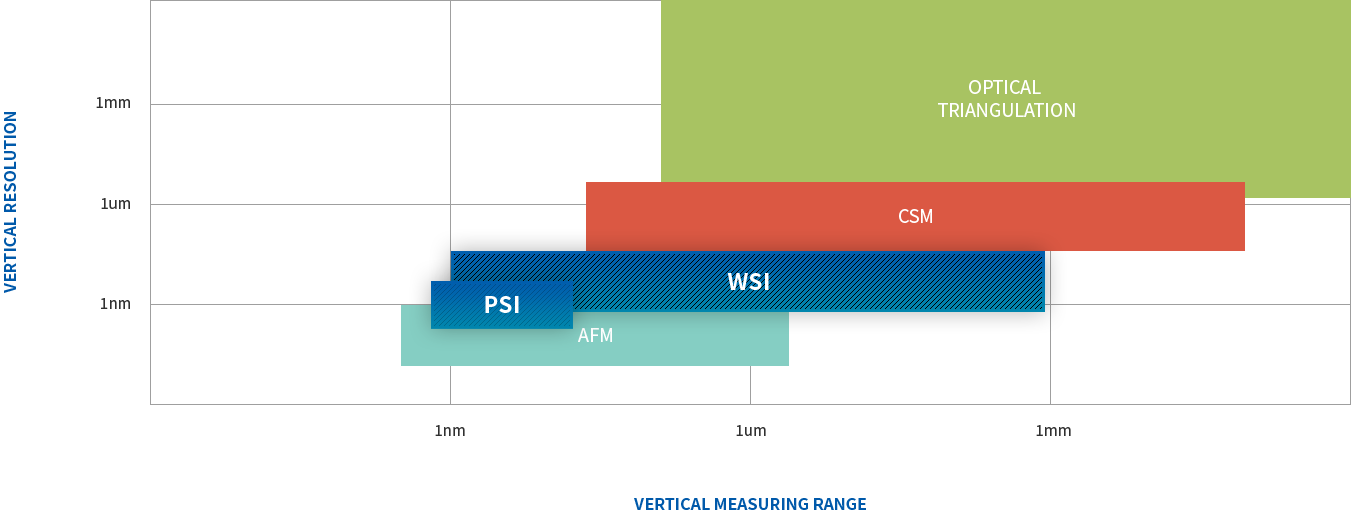
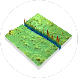
WSI measures the height of the soft surface with medium roughness and provides a vertical resolution of 0.5 nm regardless of NA. All magnifications can be used without undermining the vertical resolution.
PSI provides a vertical resolution of 0.1 nm. Thus, when a very low magnification (2.5X) is in use, a large FOV can be achieved by increasing the height resolution.
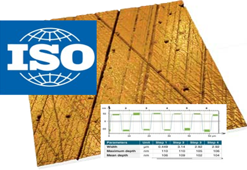
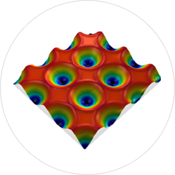
Provides various data such as roughness, height, width, etc. in a wide range of formats including graphs, excel and 2D•3D images in compliance with the standard set by ISO, the international organization for standardization.

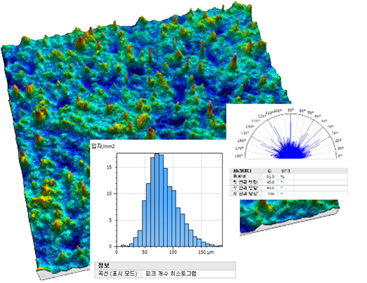
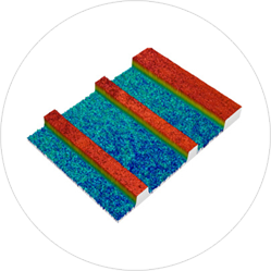
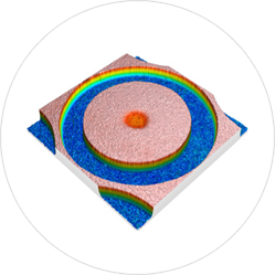
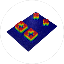
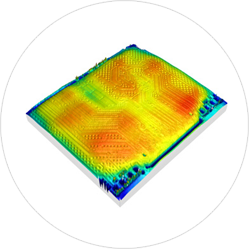
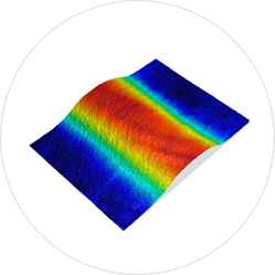
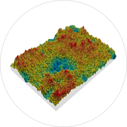
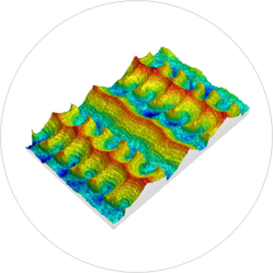
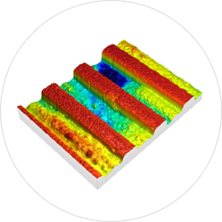
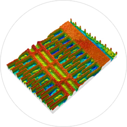
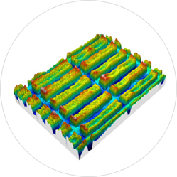
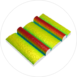
In general, the natural or manufactured surfaces generate basic images (2D•3D) with various structures, wave patterns and degrees of roughness.

Users can obtain such data according to various parameters such as critical dimensions, step height, peak-to-valley, volume and grade.
NanoSystem has over 30 roughness parameters in place, obtained from various international organizations for standardization including ISO, ASME and EUR, which can be used to evaluate roughness of samples.
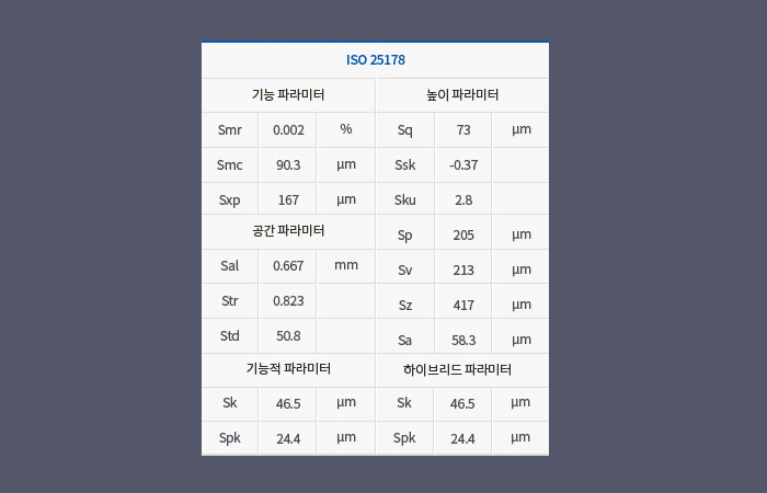
NanoSystem complies with ISO 25178.
Users can choose roughness parameters perfectly customized for them including height, space, hybrid, functions and capacity parameters.
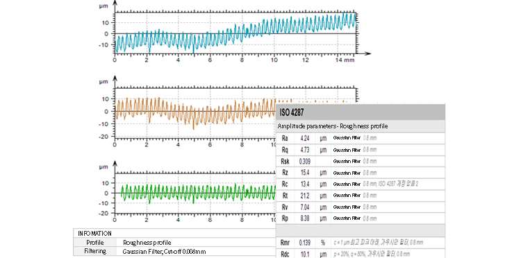
Provides 2D measurement analysis data and parameters in compliance with ISO 4287.
NanoSystem provides a variety of profiles including distance, height, valley, peak pattern, fractal analysis, texture isotropy and Abbott curve, enabling efficient data management.
Provides a variety of profiles
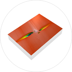
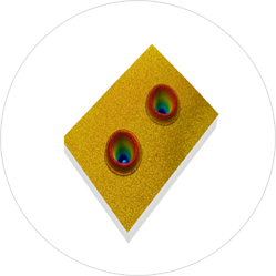
Dimple
Trace
Pad
Metal mask
MCP unit
Glass defect
OLED pattern
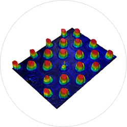
Bump on BGA
Laser marking on wafer
Engineering·Optical·Precision Parts
Copper roughness
Ball end mill
COG decap
MEMS
Nuclear pipe
MLCC
Micro lenses
Film scratch
Organic pattern
이메일주소 무단수집을 거부합니다.
본 웹사이트에 게시된 이메일 주소가 전자우편 수집 프로그램이나 그 밖의 기술적 장치를 이용하여 무단으로 수집되는 것을 거부하며, 이를 위반시 정보통신망법에 의해 형사 처벌됨을 유념하시기 바랍니다.